In the semiconductor manufacturing sector, abnormal chip stacking is a severe production issue. Unexpected stacking of chips during the manufacturing process can lead to equipment damage and process failures, and may also result in the mass scrapping of products, causing significant economic losses for enterprises.

With the continuous refinement of semiconductor manufacturing processes, higher demands are placed on quality control during production. Laser displacement sensors, as a non-contact, high-precision measurement technology, provide an effective solution for detecting chip stacking abnormalities with their rapid and accurate detection capabilities.
Detection Principle and Anomaly Judgment Logic
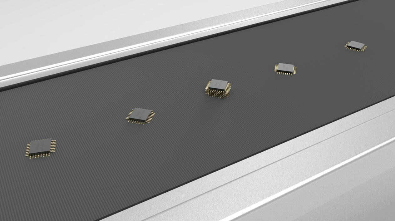
In the semiconductor manufacturing process, chips are typically placed on carriers or transport tracks in a single-layer, flat arrangement. At this time, the height of the chip surface is a preset baseline value, generally the sum of the chip thickness and the carrier height. When chips are accidentally stacked, their surface height will significantly increase. This change provides a crucial basis for detecting stacking abnormalities.
Transport Track Stacking Detection
Transport tracks are critical channels for chip movement during the manufacturing process. However, chips may accumulate on the tracks due to electrostatic adsorption or mechanical failures during transport, leading to track blockages. Such blockages can not only interrupt production flow but also damage chips.
To monitor the unobstructed flow of transport tracks, laser displacement sensors can be deployed above the tracks to scan the height of the track cross-section. If the height of a localized area is abnormal (e.g., higher or lower than the thickness of a single layer of chips), the sensors will determine it as a stacking blockage and trigger an alarm mechanism to notify operators for timely handling, ensuring smooth production flow.
Detection Process
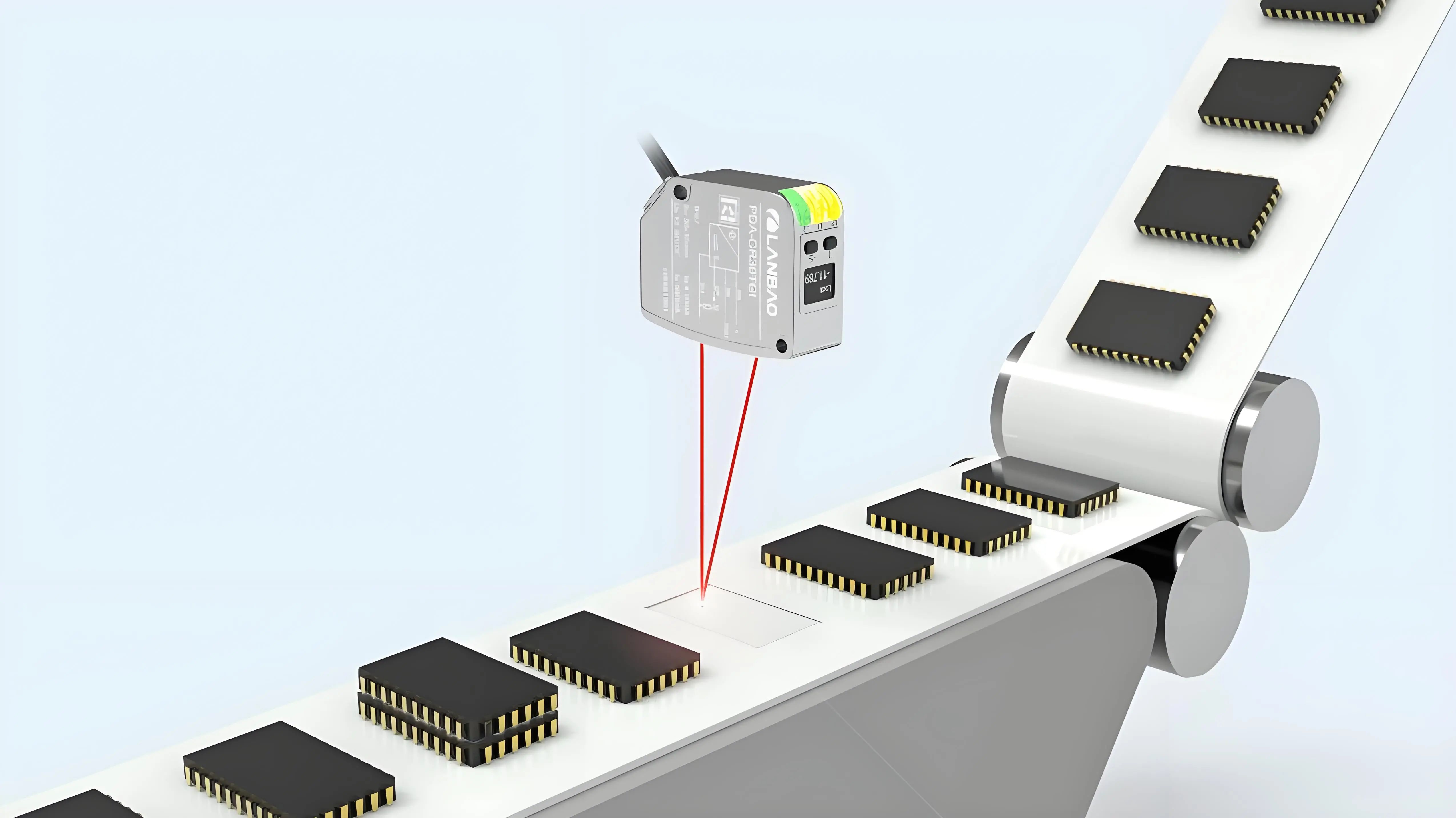
Lanbao laser displacement sensors accurately measure the height of target surfaces by emitting a laser beam, receiving the reflected signal, and utilizing the triangulation method.
The sensor is vertically aligned with the chip detection area, continuously emitting a laser and receiving the reflected signal. During chip transport, the sensor can acquire real-time surface height information.
The sensor employs an internal algorithm to compute the chip surface height value from the acquired reflected signal. To meet the high-speed transfer demands of semiconductor production lines, this necessitates that the sensor possess both high precision and a high sampling frequency.
An allowable height variation range is set, typically ±30 µm from the baseline height. If the measured value exceeds this threshold range, it is determined to be a stacking abnormality. This threshold determination logic can effectively differentiate between normal single-layer chips and stacked chips.
Upon detection of a stacking abnormality, the sensor triggers an audible and visual alarm, and simultaneously activates a robotic arm to remove the abnormal location, or pauses the production line to prevent further deterioration of the situation. This rapid response mechanism minimizes losses caused by stacking abnormalities to the greatest extent.
Real-time, high-precision detection of chip stacking abnormalities using laser displacement sensors can significantly improve the reliability and yield of semiconductor production lines. With continuous technological advancements, laser displacement sensors will play an even greater role in semiconductor manufacturing, providing strong support for the industry's sustainable development.
Post time: Mar-25-2025